How To Make A Pcb Schematic
Pcb layout design with proteus How to design a pcb layout Pcb schematic demodulator
How to Convert PCB to Schematic Diagram? - RAYMING PCB
Pcb make schematic making custom part Pcb simple layout etching diy circuit board bot drawing thoughts schematic eagle offer tips use some Pcb schematics restore raypcb protel orcad
Pcb easyeda circuit logging circuits
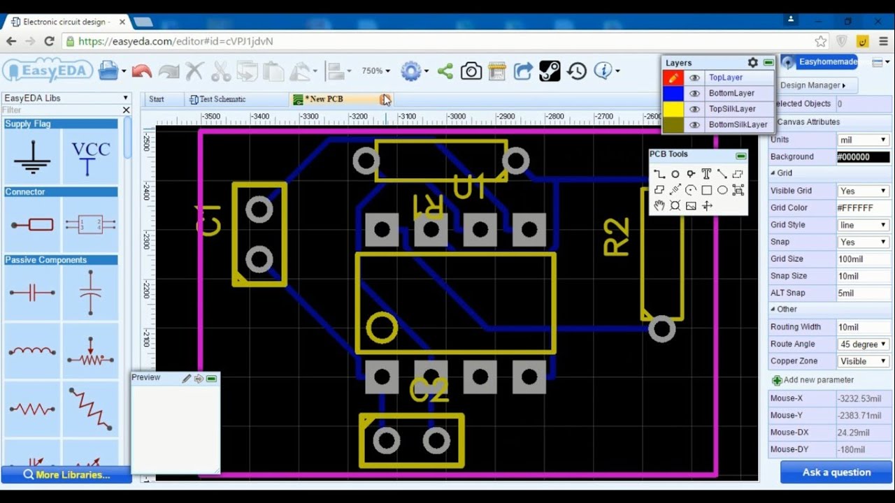
Schematic pcb altium designedComplete pcb designing tutorial using easyeda pcb design tool How to design a pcb layoutEsp8266 pcb relay.
Pcb altium schematic schema outline control creare uno databases improves convertHome wiring diagram software apk Schematic schematicsPcb layout cad schematic review do designing e2e ti basics improve efficiency file allpcb capture pcbs.

[review] my first pcb schematic design
Pcb schematic make convert layout symbol custom circuit project basics footprints associated automatically editor each willMastering the art of pcb design basics Pcb mac easyeda gadgetsFrom idea to schematic to pcb.
Circuit board class printed instructables custom online prototypePcb layout schematic connection wires How to design a pcb layoutHow to make a custom pcb.

Circuits mastering checks protoexpress
Proteus circuitSchematic fiverr Pcb schematic make layout blank custom draw circuit canvas whereHow to design a pcb layout.
Pcb layoutPcb design: how to create a printed circuit board from scratch Schematic and pcb designHow to do a pcb layout review.

Teach you how to draw a simple pcb schematic in seven steps – so good
Electronic devices & pcb development services — kickr design®Bot thoughts: simple diy pcb etching Pcb designHow to convert pcb to schematic diagram?.
How to create a pcb layout from a pcb schematic in altium designerPcb schematic easily idea do Free online circuit board design classMake pcb design pcb layout and schematic design at low cost by.

Pcb wiring audio komatsu
Circuit circuits schematic schematics electronic scratch rules think .
.


How to Convert PCB to Schematic Diagram? - RAYMING PCB
Home Wiring Diagram Software Apk
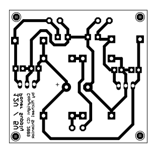
Bot Thoughts: Simple DIY PCB Etching

Free Online Circuit Board Design Class - Instructables

pcb design - PCB Layout of a circuit - Electrical Engineering Stack

How to Design a PCB Layout - Circuit Basics

Schematic and PCB Design | Danalog